Revolutionising computer tomography with photon counting
Computer tomography (CT) is indispensable in modern medicine, but CT scanners could achieve so much more with better imaging and less X-ray exposure. In a project with industrial partner ams International AG, ETH researchers are testing new materials for the promising photon counting method.
CT scanners have been around for a long time and are a reliable diagnostic tool in developed countries. Over time, various improvements have been introduced to reduce the X-ray dose and improve image quality by reducing detector noise. These can be further optimised with the photon counting method, which is based on the direct detection of X-ray photons with energy-level resolution. The method was developed more than a decade ago, and clinical trials have demonstrated its ability to improve diagnostics. However, the existing photon-counting CT systems have not yet been adopted by the market due to the very high cost and reduced technological efficiency of the detection material used.
New materials for Photon Counting Detectors
Existing photon-counting CT systems used for clinical trials use either cadmium telluride or cadmium zinc telluride as the detection material. These materials are costly due to the low yield of the detector material, the complicated manufacturing process, and the complex system integration.
The Kovalenko group at ETH has recently introduced lead halide perovskites as a promising radiation detection material that could solve the cost issues of existing photon-counting CT systems. The perovskites combine high stopping power with efficient charge transport and easy fabrication, which are distinct advantages over the current materials.
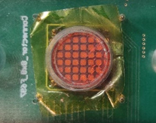
In 2020, the KovalenkoLab established the SynMatLab (Laboratory for Multiscale Materials Synthesis and Hands-on Education). It includes a state-of-the-art crystal growth facility (Bridgman growth ovens) and related equipment for single-crystal cutting, polishing, and metal contact deposition. The figure below shows the results of a grown crystal and pixelated detector made from such crystals, produced on the equipment of the SynMatLab. The world-class facility played a key role in the progress of the development of novel materials for radiation detection.
Fruitful cooperation for both sides
The COVID pandemic and the resulting need for numerous CT scans have painfully highlighted the need for photon-counting CT scanners with lower radiation exposure. Therefore, there is an urgent need to develop the photon counting method to make it more accessible. When ams International, a leading manufacturer of sensors and emitters with a large R&D centre in Rapperswil, Switzerland, read about Professor Kovalenko’s perovskite research, they contacted him to investigate the possibility of using the new materials in photon-counting CT systems.
Initial Zoom meetings led to a research collaboration supported by Innosuisse. The project started three years ago and will end in December 2024. The partners aim to make photon-counting CT a success. This will be achieved by reducing the price of the detection material and simplifying the assembly scheme, as well as reducing the X-ray dose to the patient or improving the resolution of the images.
So far, promising progress has been made and both parties are confident they will achieve their goals. While ams points out that they benefit from ETH’s knowledge in the field of detection materials, the researchers appreciate the practical and meaningful aspects of their work as well as the pragmatic support from ams.
Learnings and applications
In addition to its use in photon-counting CT systems, the researchers point out that the new material in the form of nanocrystals could also revolutionise other fields such as TV screens or computer displays. It is also a promising material for the semiconductor industry, for example, for photo cameras.
Both partners are confident that they will achieve their goals by the end of the project. The product will then have to be benchmarked against current solutions, brought into mass production, and commercialised. ams International hopes to see the new generation of photon-counting CT systems on the market in a few years.
Contact/Links:
ETH Zürich Kovalenko Lab – Functional Inorganic Materials
external pageAms International AG, Sensor Solutions
Do you want to get more "News for Industry" stories?
external pageFollow us on LinkedIn
Are you looking for research partners at ETH Zurich?
Contact ETH Industry Relations